A new world in electronic materials
Next-generation semiconductor devices for computing
High-performance IGZO transistors; ferroelectric materials and memory devices; neuromorphic devices; p-type material exploration and CMOS devices.
Amorphous Oxide Semiconductor (AOS)
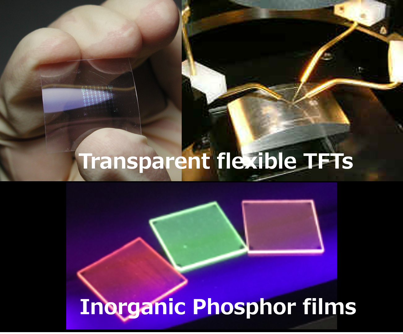 In 2004 and before, it had been believed “good semiconductor” can be realized only in crystalline materials such as Si, GaN, and ZnO. Notwithstanding that, we demonstrated the high-performance thin-film-transistor (TFT) can be realized by amorphous oxide semiconductor “IGZO”, In-Ga-Zn-O. Although “IGZO” has an amorphous structure, transparent flexible high-performance TFT can be produced. Our IGZO TFT is already in mass production in iPad, Surface Pro4, and 77-inch OLED TVs. In addition, we recently succeeded to demonstrate room-temperature fabrication of inorganic light-emitting semiconductor films, which will be used for optical devices and displays, replacing OLED in the future.
[Ref.] K. Nomura et al., Nature (2004), Science (2003)., K. Ide et al., Appl. Phys. Lett. (2022).
Realizing materials once thought impossible
Ultrawide gap amorphous oxide semiconductor
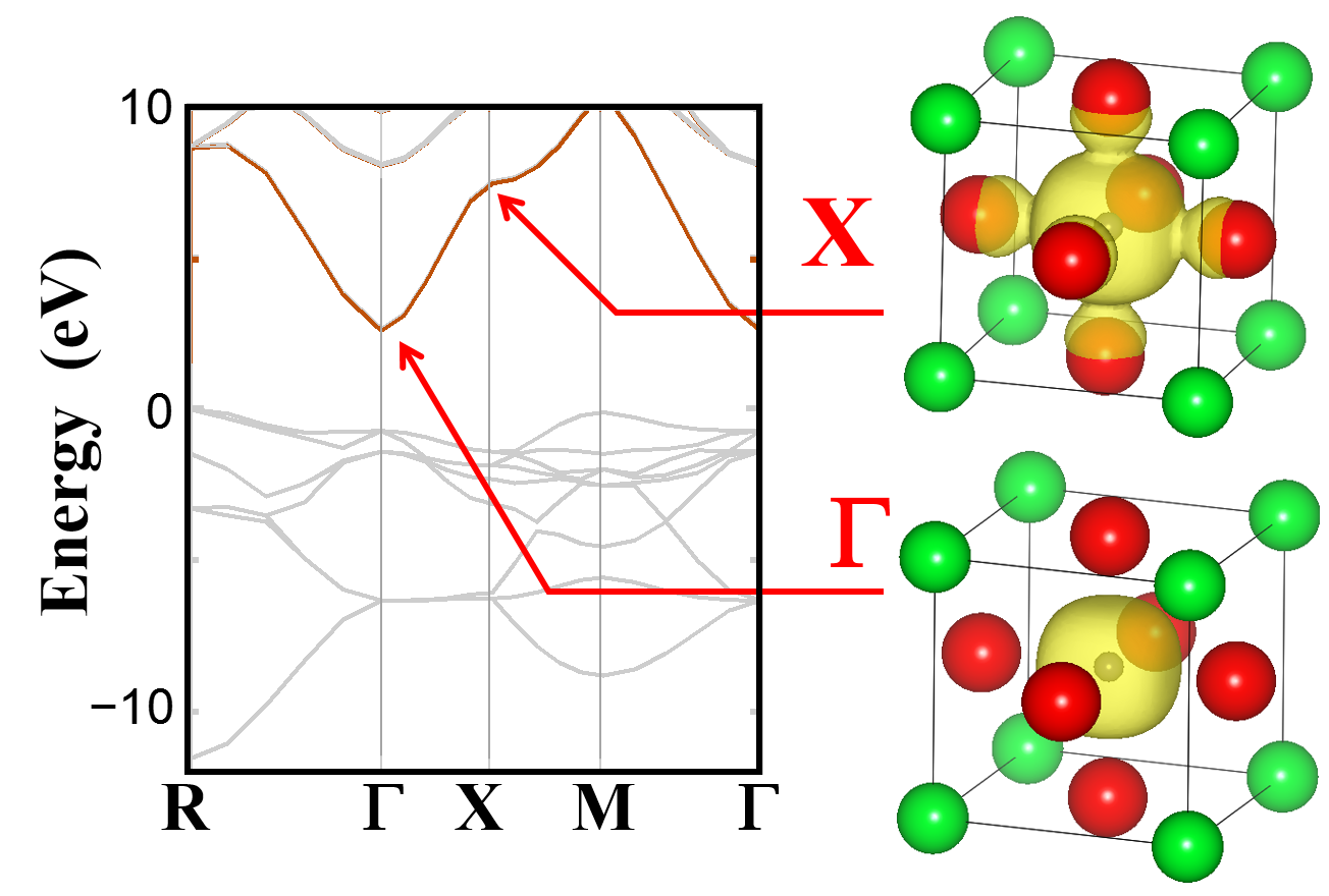
 As explained above, it had been believed the AOS does not have good electronic properties, but we then overturned this misunderstanding by IGZO TFTs. Next our target is ultrawide gap AOSs, which has been believed not to been realized until now. We recently realized GaOx AOS with a large bandgap of 4.12 eV by controlling the defects and understanding the doping mechanism in AOSs.
[Ref.] J. Kim et al., NPG Asia Mater. (2017).
Sensors, ultrawide-gap semiconductors, and environmental devices
Gas sensors using oxide semiconductor thin films; ultrawide-gap semiconductor materials; power semiconductors; and development of low environmental-impact elements and materials. We cover sensing through power electronics in a unified way, including element strategy and lower process footprint.
Solar cells, thermoelectrics, and energy conversion devices
We work on photovoltaics and energy conversion broadly; in thermoelectrics, first-principles methods that include phonons have recently become practical at scale—a major trend. A strength of our group is combining state-of-the-art calculations with materials informatics (MI), from candidate screening to evaluation of transport properties.
Computational science, MI, AI, and materials design
Transparent conductor using covalent bonds
 Germanium oxide (GeOx) is known as a good electrical insulator with a wide bandgap over 6 eV. We demonstrated to convert SrGeO3 to a good transparent conductor. Quantum calculation explains its electronic structure and why it reduce sthe bandgap down to 2.7 eV by employing the cubic SrGeO3 structure. Like this, we are making continuous challenges to create new functional materials based on our original material design concept.
[Ref.] H. Mizoguchi et al., Nature Commun. (2011).
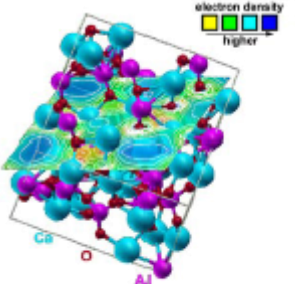 We use first-principles calculations, molecular dynamics simulations, device simulations, etc for designing our new materials and also for revealing the underlying mechanism of their functions. It is usually difficult to find new materials, but we challenge to develop novel functional materials by understanding “why the material show good properties”, predicting “how we can improve the material properties”, and confirming the idea experimentally. One of our approaches is shown in the electron density map of 12CaO・7Al2O3 (C12A7) with 0.4nm-size cage. Usually, electrons in the conventional semiconductor conduct through the positions of atoms, but for C12A7, the electrons pass through the cages, which can be visualized by the quantum calculation. By collaboration of experiment and theory, we always try to understand the underlying mechanisms and to find a way to develop novel functional materials.